
Dry Laser Cleaning
Dry laser cleaning semiconductor is a precise and contact-free method for removing contaminants such as grease, dust, or polymer residues without damaging the underlying material. It offers a clean, non-abrasive alternative to traditional chemical or mechanical processes. Femtum’s solution is based on worlds first and only 2.8 µm pulsed mid-infrared fiber laser, optimized for selective cleaning of semiconductor and optical components. The system combines high precision with easy integration into automated manufacturing environments.
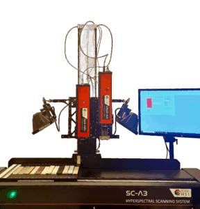
Hyperspectral Semiconductor Analysis
Our Hyperspectral Semiconductor Analysis solution combines hyperspectral imaging (HSI) with line-scan spectral ellipsometry to deliver powerful, non-destructive inspection capabilities for semiconductor wafers and thin films. This dual-technique platform enables both macro- and microscopic analysis for defect detection and material characterization.
This platform is ideal for semiconductor manufacturers aiming to improve yield, optimize thin-film processes, and enhance material quality control at every step.
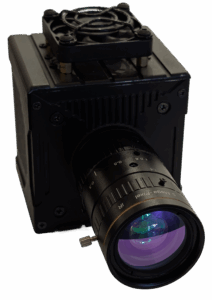
Quantum Dot‑Powered SWIR Imaging
Our Quantum Dot–Powered SWIR Imaging system leverages state‑of‑the‑art colloidal quantum dot (QDot) sensors to unlock short‑wave infrared (900–1700 nm+) capabilities at a fraction of the cost of traditional InGaAs cameras. Designed for seamless integration into semiconductor fabs, this compact solution provides true sub‑surface visualization, essential for inspecting backside wafers, 3D IC bonds, micro‑cracks, and embedded particles.