Feel free to reach out if you have any questions or need help!
Romero Kicken
+31 85 080 5944 - Option 2
romero@photonmission.com
Macro- and Microscopic Measurements for Semiconductor Analysis
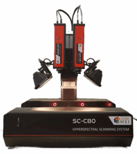
In the ever-evolving world of semiconductor manufacturing, understanding materials at both the microscopic and macroscopic levels is critical. Our Hyperspectral Semiconductor Analysis platform brings together two cutting-edge technologies—hyperspectral imaging (HSI) and line-scan spectral ellipsometry—to enable precise, non-destructive inspection across a broad range of semiconductor materials. Rather than relying on isolated data points or limited field-of-view inspection methods, HSI captures both spatial and spectral information simultaneously. This allows for in-depth analysis of complex wafer surfaces, detecting features such as pinholes, inclusions, micro-cracks, and roughness variations with exceptional clarity. Whether you’re working with silicon, GaAs, InP, GaN, or other compound semiconductors, the system adapts to the unique spectral signatures of each material—capturing signals from electroluminescence, photoluminescence, reflection, and transmission within a spectral window spanning 250 to 1700 nm. Where HSI maps the surface with speed and precision, line-scan spectral ellipsometry adds another layer of insight—measuring thin-film thicknesses, refractive indices, and optical constants with sub-nanometre accuracy. This polarization-based technique provides critical information about uniformity and layer composition, enabling manufacturers to optimize deposition processes and verify device integrity without physically touching the sample. Together, these technologies overcome traditional limitations. Line-scan HSI provides high-throughput coverage over large areas, while the spectral ellipsometer offers detailed measurements at the layer level—far beyond what conventional confocal systems can achieve on their own. While high-resolution imaging can require advanced data processing capabilities, the results offer unmatched value for both R&D and industrial-scale quality control. Designed for semiconductor inspection environments where speed, resolution, and material specificity are all essential, our solution delivers a powerful, integrated approach to wafer and film analysis—one that keeps pace with the growing demands of modern electronics manufacturing.

Check out our Hyperspectral Imaging Systems
Clyde HSI is on a mission to provide each and every one of their clients with a complete, end-to-end hyperspectral imaging solution. Each solution is designed and rigorously tested to ensure robust, reliable, accurate and repeatable hyperspectral imaging measurements across a range of academic and industrial applications.
We believe that their high quality engineering and design, allows them to develop market leading products and services. Within our Photonics Research Facility, they have the capability to rapidly develop new products and systems, and welcome the opportunity to partner with our customers on new developments - both within the scientific research community and for equipment for industrial applications.